3D Integration
Integrated systems at the nanoscale regime face increasing challenges related to manufacturing, design, and packaging. The main thrust of the semiconductor evolution, which is to scale the physical dimensions of the devices is predicted to decelerate as further device miniaturization results in less predictable physical behavior, decreasing reliability, and skyrocketing manufacturing costs. In addition, fundamental physics determines with (discomforting) precision the ultimate scaling boundaries. The growing unreliability and unpredictability of the semiconductor devices combined with gigascale integration densities complicate the design process of contemporary VLSI systems. The increasing power and escalating number of input/output connections to the outside world also set stringent demands on the package design for these systems.
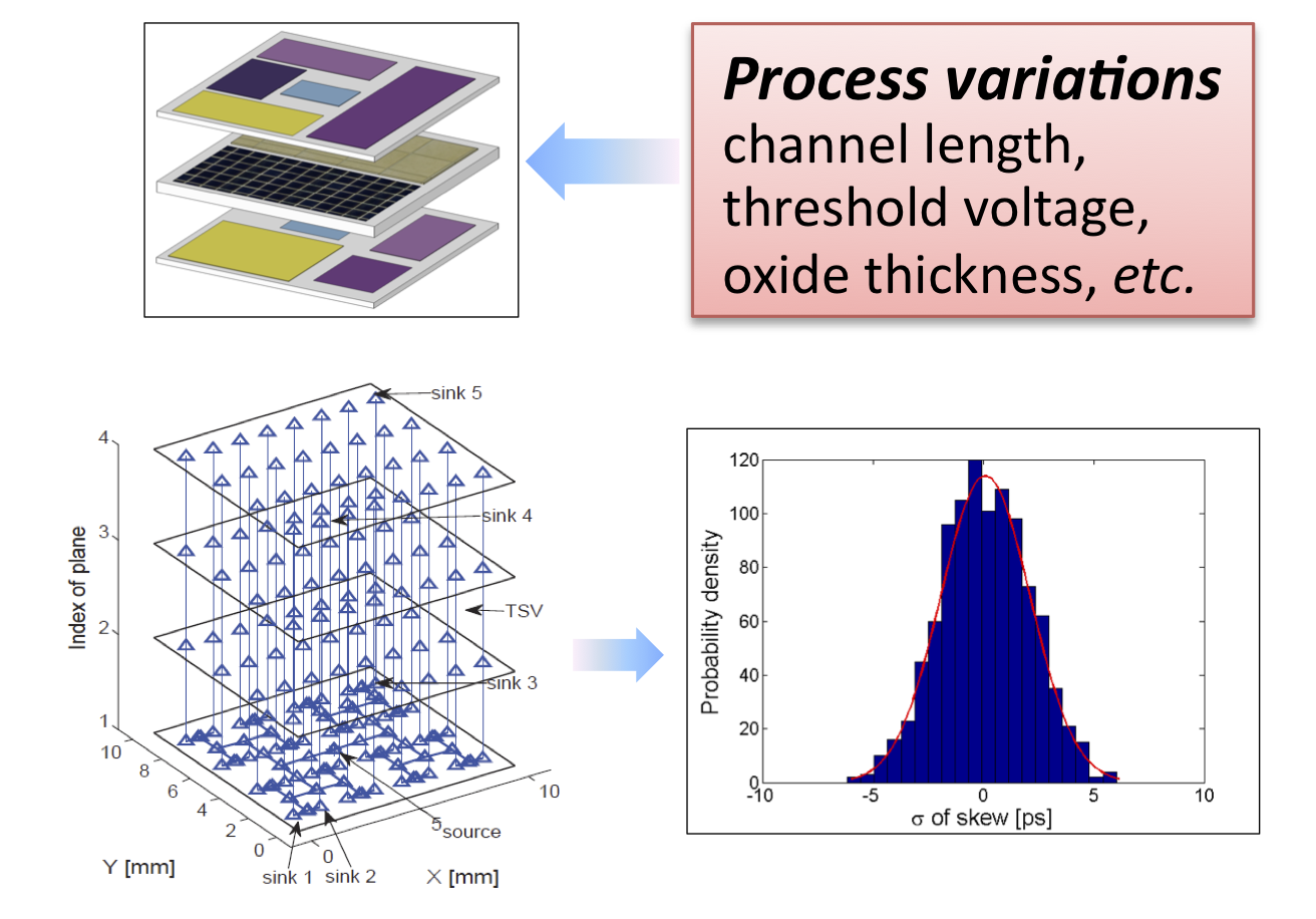
To respond to these multiple objectives, disruptive solutions that provide considerable improvements, while employing mature fabrication processes and the existing manufacturing infrastructure, are required. A promising design and packaging paradigm is three-dimensional (3-D) or vertical integration. Utilizing the third physical dimension as a means to integrate more and different functions can greatly expand the capabilities of envisaged computing and sensing systems. In a three-dimensional system, the requirement for higher integration density is served by bonding several conventional (planar) circuits electrically connected with short vertical wires. The development of 3-D systems with multiple logic and memory layers interconnected with high-density fine-grain vertical wires is the ultimate goal of the investigated 3-D technologies.
To this end, many design tasks should be addressed. For example, power becomes the predominant constraint as compared to planar circuits due to the reduced footprint of 3-D circuits. Interconnect design also introduces new problems related to the vertical interconnects that are now required. Moreover, the 3-D nature of these systems complicates the design process for the global circuit infrastructure, such as the clock and power distribution networks. To address these design issues, novel approaches to model and analyze the behavior of highly compact 3-D systems are, consequently, required. The research activities on 3-D integration within LSI emphasize physical design models to analyze the behavior of these systems, design methodologies and algorithms to enable the development of 3-D circuits, and exploratory design tools to leverage the fast progress of this emerging and highly potent technology.