CAD for Nanosystems
3D Integration provides an effective platform for realizing nanosystems. We are researching – in cooperation with CEA/LETI – 3D monolithic integration, where the stacked active layers are processed sequentially and where the 3D contacts in the order of few 100 nanometers. This technology differs from the standard die-stacking technique using through-silicon vias, which are 10X bigger in size. In 3D monolithic integration, the benefits in terms of wirelength, latency and power depend on the granularity level at which the circuit is partitioned. In monolithic 3D integration, transitors can be superimposed in the vertical direction, thus achieving a tight packing of functionality. Figure 1 illustrates circuit partitioning with various granularities. At a coarse-grain level, we can have cache on top of cores, or cores on top of cores, as presented in Figure 1a. At a finer level of granularity we can realize functional blocks on top of each other (Figure 1b). Going at even finer level, we can perform 3D stacking at the gate and standard cell level, as illustrated in Figure 1(c,d). Consequently, 3DMI is an ideal choice for ultra-high density 3D circuits.
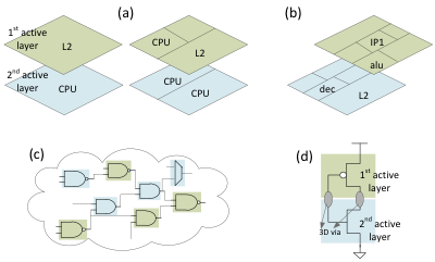
Figure 1. Circuit partitioning with various granularities
We have developed a new design technique for realizing fine-stacking at the transistor/gate level and corresponding CAD tools (INTRACEL and CELONCEL). With INTRACEL, planar standard cells are transformed into 3D cells by realizing the pull-up network and pull-down network in two different active layers (Figure 1d). With CELONCEL, standard cells are designed such that they can overlap with the cells at the bottom or with the cells on the top active layer (Figure 1c). The logic-to-layout design flow for both the transformations is presented in the figure below. The design technique proposed in this work is compatible with the VLSI processing and has minimal impact on existing VLSI design flows.
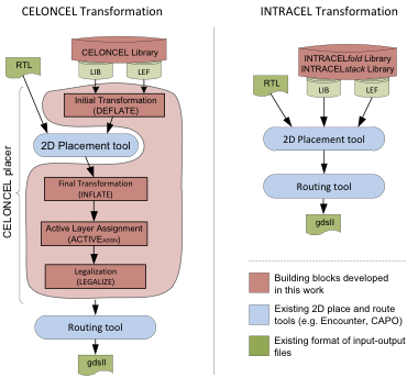
Figure 2