Contact:
Haykel Ben Jamaa, PhD Student, EPFL-IC-LSI
Partners:
STMicroelectronics, Post-Silicon Technology, Milan, Italy
Microelectronics Systems Laboratory (EPFL-STI-LSM), Lausanne, Switzerland
Keywords: Nanotechnology, silicon nanowires, crossbar memories, RAM, reliability, addressing
Presentation:
The scaling process of the already fifty years old Complementary Metal-Oxide-Semiconductor (CMOS) technology is still in progress and will probably keep on providing the semiconductor market with smaller devices and more complex chips for the next decades. However, reducing the device size down to few tens of nanometer is becoming tough for device, circuit and mask designers. The recent development of bottom-up techniques allowing the fabrication of nano scale wires (nanowires and -tubes) and molecular switches raises the idea of combining these techniques with classical top-down VLSI approaches. The final goal is to achieve a higher integration while keeping the costs low enough. The bottom-up techniques are compatible with regular CMOS architectures such that crossbars, and the final product is a highly integrated hybrid crossbar circuit. This combination necessitates novel architectural paradigms in order to achieve reliable systems and fill the gap between the lithographic dimensions and the nanometer scale devices.
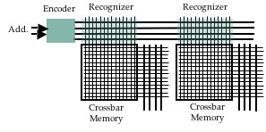
Baseline Architecture of Crossbar Memories
Goal:
The guideline of this project is to fabricate a prototype of a reliable nanometer scale crossbar circuit in a standard CMOS process despite the photolithographic limitations, performing the function of a Random Access Memory (RAM), storing the information in molecular switches and extensible to a logic circuit. The reliability issue will be addressed at two different levels: on the one hand, by optimizing the process; on the other hand, by adding redundancy with different granularities at the circuit level. The nano-to-micro gap will be filled by adapted addressing techniques. The architectural approach can be generalized to other underlying technological assumptions.
Publications:
“Improving the Fault Tolerance of Nanometric PLA Designs”, Federico Angiolini, M. Haykel Ben Jamaa, David Atienza, Luca Benini, Giovanni De Micheli; in Proceedings of Date ’07
Click here to see a complete publication list.
Download project description file (88 KB pdf)