![]()
People
 |
Pierre-Emmanuel Gaillardon Post-doctoral Researcher Emerging device technologies |
|
 |
Luca Amaru PhD Student EDA tools |
PhD project page: Electronic Design Automation for Emerging Technologies and Applications |
 |
Michele De Marchi PhD Student Controllable-polarity |
PhD project: Fabrication of Double Gate Silicon Nanowire FETs with run-time Polarity Control |
 |
Hassan Ghasemzadeh PhD Student Reliability |
PhD project page: |
 |
Jian Zhang PhD Student Controllable-polarity |
PhD project: Fabrication and Simulation of Multiple-Independent-Gate Nanowire FETs and Circuits |
Nanosystems are integrated systems exploiting nanoelectronic devices. In particular, this project considers silicon nanowire and carbon nanotube technologies as replacement/enhancement of current silicon technologies. The broad objective of this project is to study system organization, architectures and design tools which, based on a deep understanding and abstraction of the manufacturing technologies, allow us to realize nanosystems that outperform current integrated systems in terms of capabilities and performance. Thus this project will address modelling of technological aspects, synthesis and optimization of information processing functions from high-level specifications into the nanofabric, and new design technologies for specific aspects of nanosystems including, but not limited to, sensing and interfacing with the environment. This project will address also cross-cutting design goals such as ultra-low power and high-dependability design, with the overall objective of realizing nanosystems that are autonomous (w.r. to energy consumption) and autonomic (i.e., self healing).
General objectives
Much of our economy and way of living will be affected by nanotechnologies in the decade to come and beyond. Mastering materials at the molecular level and their interaction with living matter opens up unforeseeable horizons. This project deals with how we conceive, design and use nanosystems, i.e., integrated systems exploiting nanodevices. Whereas switching circuits and microelectronics have been the enablers of computer and communication systems, nanosystems have the potentials to realize innovative computational fabrics whose applications require broader hardware abstractions, extended software layers and with a much higher complexity level overall. The abstraction of computation, the nanosystem architecture, the technological feasibility envelope and the multivariate design optimization problems pose challenging and disruptive research questions tackled by this project.
This project addresses an important need of the European industry, where enabling creativity and diversity is important to sustain the semiconductor and systems segments. Whereas mass-production and low-cost manufacturing technologies are shifting to Asia, the design of complex multi-faceted high-value-added systems is key to retain engineering capability and productivity in Europe.
Physical and logic design
The physical implementation of nanosystems is a regular fabric of computational and storage blocks, connected by a hierarchical network. Regularity is of utmost importance as performance – such as latency through a component – is dominated by the transit time on the communication wires and not by the computational/storage functions. Hence reducing the delay spread in the geometrical structure is key to performance. Thus we envision the internal geometrical structure as a set of regular arrays. The specific filiform structure of SiNWs and CNTs supports the design of dense gate arrays and crossbars.
Within the research domain, vertically-stacked Silicon NanoWires Field Effect Transistors (SiNWFETs) [1] are a promising extension to the FinFETs. Indeed, by splitting the thin film transistor channel into a collection of 1-D structures (i.e., SiNWs), the transistor exhibits superior performance. The Gate-All-Around (GAA) structure improves the electrostatic control of the channel and leads to a higher Ion/Ioff ratio and reduced leakage current [2].
At advanced technology nodes, an increasingly larger number of devices are affected by Schottky contacts at the source and drain interfaces. Hence, devices face an ambipolar behavior, i.e., each device exhibits n- and p-type characteristics simultaneously, because of the possible flow of electron and holes in the channel. While most technologies tend to suppress this behavior through additional process steps, new design methodologies [3,4] showed that it is of high interest to control the ambipolar phenomenon through programmable polarity devices. Indeed, by engineering the source and drain contacts and by constructing independent Double-Gate (DG) structures, the device polarity can be electrostatically programmed to be either n– or p-type. The functionality of a transistor with controllable polarity is an exclusive or (EXOR) of the logic signals on both gates. Thus, the fundamental switching primitive, the DG-SiNWFET, is intrinsically more expressive in terms of logic as compared to standard (CMOS) transistors.
The ambipolar conduction phenomenon is observable in several nanoscale FET devices (45-nm node and below), including silicon [5], carbon nanotubes [6] and graphene [7]. The control of the ambipolarity allows us to adjust the device polarity online. Such transistors, i.e. with a controllable polarity, have been experimentally fabricated in several novel technologies, such as carbon nanotubes [8], graphene [9] and Silicon NanoWires (SiNWs) [10,11]. To the best of our knowledge, Sacchetto et al. [12] and De Marchi et al. [13] were the first to fabricate and test successfully SiNW transistors with independent individual control. They introduced DG-SiNWFETs where one gate controls the polarity (i.e., type of carrier, n or p) while the other gate controls the carrier flow in the channel. The operation of these FETs is enabled by the regulation of Schottky barriers on source/drain junctions through the additional gate.
In particular, De Marchi et al. [13] fabricated vertically-stacked SiNW FETs, featuring two gate-all-around electrodes (Fig. 1). Vertically-stacked GAA SiNWs represent a natural evolution of FinFET structures, providing better electrostatic control over the channel and consequently superior scalability properties [13].
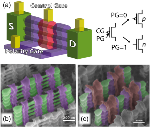
Fig. 1. 3D sketch of the SiNWFETs featuring 2 independent gates and its associated symbol (a), tilted SEM views of an array of fabricated devices before creation of the control gate (b) after addition of the polarity gates (c). S/D pillars and nanowires (green), PG (violet) and CG (red) are shown [13].
In the device, one gate electrode, the Control Gate (CG) acts conventionally by turning on and off the device. The other electrode, the Polarity Gate (PG), acts on the side regions of the device, in proximity of the Source/Drain (S/D) Schottky junctions, switching the device polarity dynamically between n- and p-type (Fig. 2). The input and output voltage levels are compatible, resulting in directly-cascadable logic gates.
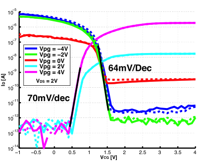
Fig. 2. IDS-VCG logarithmic plot of a measured device for several VPG voltages. Curves extracted at VDS=2V [13].
Digital circuits using these transistors can exploit both gates as inputs, thereby enabling the design of compact cells that implement XOR more efficiently than in CMOS. Indeed, in the context of digital operations, DG-SiNWFETs realize intrinsically an XOR characteristics because the transistor is ON when PG=CG, i.e.,![]() , and consequently is OFF when
, and consequently is OFF when ![]() . Fig. 3 presents a pseudo-logic XOR gate. The device in the pull-down network is polarized by means of the PG. In the case of the n-type polarization, the characteristics of a pseudo-logic inverter is obtained (green). In the p-type polarization, a buffer is obtained (blue). As shown in the inset truth table, an XOR function can be implemented by a single transistor and a pull-up.
. Fig. 3 presents a pseudo-logic XOR gate. The device in the pull-down network is polarized by means of the PG. In the case of the n-type polarization, the characteristics of a pseudo-logic inverter is obtained (green). In the p-type polarization, a buffer is obtained (blue). As shown in the inset truth table, an XOR function can be implemented by a single transistor and a pull-up.
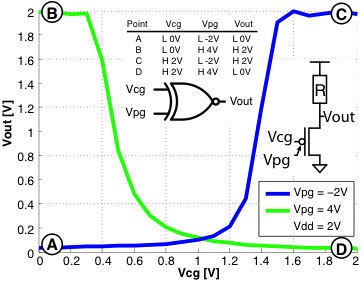
Fig. 3. Pseudo-logic XOR characteristic obtained using a single SiNWFET with controllable polarity [15].
The unique feature of this device of being polarized electrostatically was first employed to build a reconfigurable logic cell [3], and later used to define a static XOR-intensive logic family [4]. In particular, a full-swing 2-input XOR gate can be achieved by using a complementary pull-up and parallel transistors to avoid threshold drops. The XOR and XNOR implementations, reported in Fig. 4, require 4 transistors while the traditional full-swing static CMOS implementation uses 8 transistors [15].
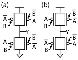
Fig. 4. 2-input XOR (a) and XNOR (b) gates build with DG-SiNWFETs [4].
Various families of logic gates can be designed for DG SiNWFETs. In particular, one can extend the principle shown in Fig. 4 to design arbitrary combinational logic functions. Alternatively, fewer transistors can be used by either employing a dynamic (or resistive) load, or by correcting the reduced swing due to threshold drops by using an output buffer. Examples of realizations of arbitrary functions are shown in Fig. 5.
Interconnect design
When taking a broader (system) look at a nanosystem, this appears to us as an ocean of components, that can be specialized to a function, or to a set of functions, by imposing a specific communication structure and protocol. A structured and layered model to achieve this purpose is by means of a multi-layered network on chip (NoC). It is general belief that NoCs will play an increasingly more important role as system complexity scales up, as in the case of nanosystems. Specifically, this project envisions nanosystems as possibly realized by superimposed slices, i.e., as three-dimensional systems (3D integration). The system integrator will mix and match slices coming from several providers, with vertical connections realized by through-silicon vias (TSVs). Thus, the NoC will provide us with a reconfigurable means to realize the vertical connectivity after manufacturing, as well as support for reliable and configurable design to match application requirements.
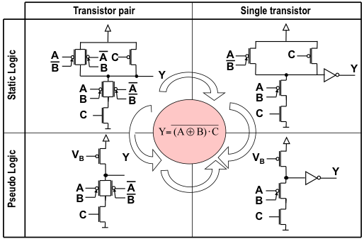
Fig. 5. Various implementions of the function ![]()
Regular layout fabrics have the advantage of higher yield as they maximize layout manufacturability. In this section, we describe a novel architecture, called sea-of-tiles (SoTs), which is an array of logic tiles that are uniformly spread across the chip. The concept is illustrated in Fig. 6. Each tile is a template that can be wired to implement an elementary logic gate, like a NOR, NAND, XOR, DFF or more generally a single-output combinational logic function. Note first that functions realized in ambipolar technology are not restricted to be unate. It is important to stress that the choice of logic tile (or tiles) to use in an array is important, as larger tiles can implement more complex functions but waste devices for smaller functions, as in the case of gate arrays.
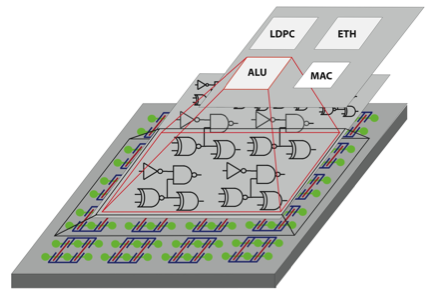
Fig. 6. Conceptual representation of a regular sea-of-tiles. Tiles are configured to realize logic functions that are part of a complex system such as a processor [14].
To enable the compact implementation of functions with the proposed transistors, we use a novel symbolic-layout technique, called dumbbell-stick diagrams [16].
Similar to the CMOS stick diagrams [17], dumbbell-stick diagrams abstract the topology of logic gates with DG FETs technology. They are a convenient means for designing compact layouts and for minimizing the cell routing complexity. Fig. 7a shows the dumbbell-stick diagram and how it is inspired by the physical shape of the device. The suspended silicon nanowires between the source and drain contacts form the basic dumbbell. The control gate and the polarity gate constitute the sticks. From this representation, we introduce the notion of transistor pairing and transistor grouping. Transistor pairing (Fig. 7b) helps in aligning the control gates of the complementary transistors in the pull-up and pull-down networks, whereas with transistor grouping (Fig. 7c) polarity gates of adjacent transistors are connected together. A logic tile is defined as an array of transistor pairs, with contiguous S/D pairs. Pairing and grouping reduce the number of input pins to the tile. A tile, consisting of two transistor-pairs grouped together is depicted in Fig. 7d. This simple tile is very effective in realizing logic primitives.
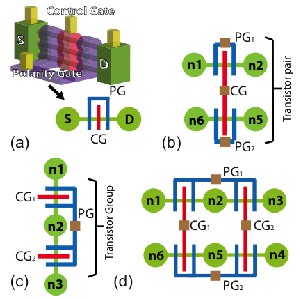
Fig. 7. Dumbell-stick diagram (a), transistor pairing (b), transitor grouping (c) and logic Tile (d).
Design
Synthesis algorithms are used to map components onto the nanofabric. Objectives include realizing blocks with verifiable functional and timing properties in spite of the presence of defects (due to the nanoscale) and failures. Whereas some known models and techniques can be used for crossbar-oriented design, now specific features of the design flow have to take into account the stochasticity of the nanofabric, where malfunctions may exist and must be isolated. Since the computational fabric is fragile and prone to fail during manufacturing and/or at run time, logic design must include redundancy and encoding so that failures can be captured (with a predefined probability objective) and be corrected by alternative means/paths of computation. Specific encoding schemes can be used to determine computational malfunctions. Moreover, the satisfaction of some timing properties, such as synchronous cycle-time constraints and timeouts, can be checked on line by shadow register techniques and their extensions. A specific characteristic of our components is the presence of low-overhead built-in detection of on-line failures and correction of soft failures.
Among on-line testing strategies, self-checking circuits offer an efficient way of testing circuits without adding redundant voter circuitry such as in Triple Modular Redundancy (TMR) [18]. The most used self-checking technique is the parity prediction scheme [19]. Parity computation relies largely on the XOR operation, and therefore its implementation with the DG-SiNWFET technology can be fairly effective. The design of a self-checking ripple-carry adder has been introduced in [20] and is shown in Fig. 8.
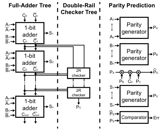
Fig. 8: Self-Checking n-bit adder using Carry-Checking Parity-Prediction scheme [19].
The adder includes 1-bit adders with complemented carry, double-rail checkers and parity generation trees. The complemented carry can be included within the existing FA structure thanks to a compact minority operator. Indeed, only 4 extra transistors are required, while static CMOS design style needs 12 extra transistors. The parity-generation tree includes cascaded compact 2-input XORs. Unfortunately the compact 4-transistor XOR implementation enabled by DG-SiNWFETs does not provide the fault-secure property. Indeed, in case of a fault on the polarity gates, there exist some conditions where all the transistors take the same polarity, therefore leading to undetermined levels at the output. For this reason, in [20], few parts of the circuit (the double-rail checkers) are still implemented using a traditional static CMOS implementation to guarantee the self-checking property. Nevertheless, the use of DG-SiNWFETs opens new opportunities also for fault-tolerant architectures.
Broadly speaking, nanosystems have to be conceived along the principles of autonomic design, in order to to achieve highly-available services in presence of local failures. In general, the nanosystem has to be cognizant of the possible local failures and of the ways of configuring itself to avoid or mitigate the consequences. Similarly, the nanosystem has to be cognizant of the possible involuntary or malicious attacks, and ways to respond to it. Nanosystems need to support graceful degradation, in case of partial failure, noisy data or poor connectivity. NoC design in nanosystems provides a layered approach to communication that can support some autonomic functions. Multi-path communication structures supports alternate means to transfer data in presence of failing links. Redundancy of computational blocks, in connection with reconfigurable networks, provides a means of supporting correct operation in spite of failing and/or defective blocks. Hence nanosystems with some manufacturing defects can be safely operated, thus augmenting the production yield and reducing the related manufacturing cost per unit.
Summary
This project addresses groundbreaking research that will enable designers to leverage new nanoelectronic technologies, such as silicon nanowires and carbon nanotubes, to manufacture integrated nanosystems. This research is challenging as it enters the uncharted territories delimited by new nanoelectronic devices and fabrics. A concerted effort at the system level, combining logic design, hardware abstraction and mapping as well as the use of formal modelling and algorithmic techniques for design automation and optimization, will make the design of integrated nanosystems a reality in the coming years. The benefits of nanosystems will go beyond a 100X increase in computational density, as new interaction paradigms, such as motion and biosensing, will enhance tremendously the capabilities of these systems in new domains and markets. The disruptive outcome of this research will be important to keep Europe at the forefront of innovation in electronics and systems, and will create new avenues for scientific research and commercial developments.
This project is supported by an ERC senior grant.
References
- S. D. Suk et al., “High performance 5nm radius twin silicon nanowire mosfet (tsnwfet): fabrication on bulk si wafer, characteristics, and reliability,” IEDM Tech. Dig., 2005.
- S. Bangsaruntip et al., “High performance and highly uniform gate-all-around silicon nanowire MOSFETs with wire size dependent scaling,” IEDM Tech. Dig., 2009.
- I. O’Connor et al., “CNTFET modeling and reconfigurable logic-circuit design,” IEEE Trans. on CAS, vol. 54, pp. 2365-2379, 2007.
- M.H. Ben Jamaa, K. Mohanram and G. De Micheli, “Novel library of logic gates with ambipolar CNTFETs: Opportunities for multi-level logic synthesis,” DATE Tech. Dig., 2009.
- A. Colli, S. Pisana, A. Fasoli, J. Robertson and A. C. Ferrari, “Electronic transport in ambipolar silicon nanowires,” phys. stat. sol.(b), vol. 244, pp. 4161-4164, 2007.
- R. Martel et al., “Ambipolar electrical transport in semiconducting single-wall carbon nanotubes,” Phys. Rev. Lett., vol. 87, 2001.
- A. K. Geim and K. S., Novoselov, “The rise of graphene,” Nature Materials, vol. 6, pp. 183-191, 2007.
- Y.-M. Lin, J. Appenzeller, J. Knoch and P. Avouris “High-Performance Carbon Nanotube Field-Effect Transistor With Tunable Polarities,” IEEE Trans. Nanotechnology, vol. 4, pp. 481-489, 2005.
- N. Harada, K. Yagi, S. Sato and N. Yokoyama, “A polarity-controllable graphene inverter,” Applied Physics Letters, vol. 96, pp. 12102, 2010.
- J. Appenzeller, J. Knoch, E. Tutuc, M. Reuter and S. Guha, “Dual-gate silicon nanowire transistors with nickel silicide contacts,” IEDM Tech. Dig., 2006.
- A. Heinzig, S. Slesazeck, F. Kreupl, T. Mikolajick and W. M. Weber, “Reconfigurable Silicon Nanowire Transistors,” Nano Letters, vol. 12, pp. 119-124, 2011.
- D. Sacchetto, G. De Micheli and Y. Leblebici, “Ambipolar Gate-Controllable SiNW FETs for Configurable Expressive Capability,” IEEE Electron Device Letters, vol. 33, num. 2, pp. 143-145, 2012.
- M. De Marchi et al., “Polarity control in Double-Gate, Gate-All-Around Vertically Stacked Silicon Nanowire FETs,” IEDM Tech. Dig., 2012.
- P.-E. Gaillardon et al., “Vertically Stacked Double Gate Nanowires FETs with Controllable Polarity: From Devices to Regular ASICs,” DATE Tech. Dig., 2013.
- J.M. Rabaey, A.P. Chandrakasan and B. Nikolic, “Digital Integrated Circuits: A Design Perspective,” Prentice Hall, 2003.
- S. Bobba, M. De Marchi, Y. Leblebici an G. De Micheli, “Physical Synthesis onto a Sea-of-Tiles with Double-Gate Silicon Nanowire Transistors,” DAC Tech. Dig., 2012.
- N. Weste and D. Harris, “CMOS VLSI Design: A Circuit and Systems Perspective,” Addison Wesley, 2004.
- P. Graham and M. Gokhale, “Nanocomputing in the Presence of Defects and Faults: A survey,” Nano, Quantum and Molecular Computing, Springer, 2004.
- M. Nicolaidis, “Efficient implementations of self-checking adders and ALUs,” Symp. On Fault-Tolerance Comput., 1993.
- O. Türkyilmaz, L. Amarù, F. Clermidy, P.-E. Gaillardon, G. De Micheli,”Self-Checking Ripple-Carry Adder with Ambipolar Silicon Nanowire FET,” ISCAS Tech. Dig., 2013.
Embed of video is only possible from Mediaspace, SwitchTube, Vimeo or Youtube