***Archived: This is a past project, it is not on offer at the moment!***
Project Description:
Variations in integrated circuits are manifested as environmental and process deviations of the characteristics of the transistors and the wires. An environmental source of variation is the fluctuation of the supply voltage (Vdd). This fluctuation directly affects the performance of the circuit resulting typically in an increase in the delay of those paths that are subjected to this fluctuation. If uncontrolled, this type of variation can result in significantly degraded circuit performance, reducing, in turn, the yield of the circuit. Significant design effort and ancillary means, such as decoupling capacitors, are employed to limit the magnitude and frequency of this noise.
 |
 |
|
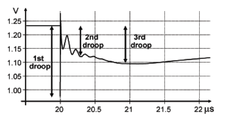
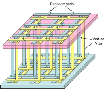
| Fig. 1. Power supply fluctuation due to circuit switching (K. L. Wong, T. Rahal-Arabi, M. Ma and G. Taylor, “Enhancing Microprocessor Immunity to Power Supply Noise With Clock-Data Compensation,” IEEE Journal of Solid-State Circuits, Vol. 41, No. 4, pp. 749-758, April 2006). | Fig. 2. An example of a power grid in a two-layer 3-D circuit. |
In 3-D circuits where the footprint of a circuit can considerably be reduced and fewer package pins are available for power and ground, power supply noise can greatly increase as compared to planar circuits. The behavior of this noise source for 3-D circuits, however, has not sufficiently been investigated and understood. The purpose of this project, consequently, is to dedicate the proper effort to analyze this type of noise in multi-layer circuits.
The project will include the following steps, 1) some reading on power supply noise and power distribution networks, 2) synthesis of different 3-D power network structures with Cadence, 3) extensive simulations to described the noise behavior within these designs, and 4) analytic modeling of the power supply noise within the context of variational analysis of multi-layer circuits (the 4th step will be implemented only if the project is assigned as a master thesis project).
The eligibility requirements for this project are
- VLSI design I and II (EE 431)
- Knowledge of Cadence (schematic entry and analog design environment)
This project was supervised by Vasilis Pavlidis and Hu Xu.
***Archived: This is a past project, it is not on offer at the moment!***