Thesis title: Design Methodologies and CAD for Emerging Nanotechnologies
Year: 2013
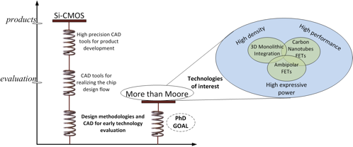
On Design Methodologies and CAD for “More than Moore” Technologies
Contact Person:
Shashikanth Bobba ([email protected]), EPFL-IC-LSI
Partners:
Robust Design Group (Prof. Subhasish Mitra); Stanford University
CEA-LETI (LDI and LTPI); Grenoble
Microelectronics Systems Laboratory (Prof. Yusuf Leblebici); EPFL
Keywords:
Nanotechnology, Silicon nanowires, Carbon nanotubes, 3D, Monolithic Integration, Ambipolar, transistors, Defect-tolerant design style
Download project description file (241 KB pdf)
Abstract:
Foreseeing the trends dictated by Moore’s law and anticipating the fundamental limits of CMOS technology in the near future, the semiconductor industry is in a quest for a successor technology to CMOS. Among the technologies being considered, “More than Moore” technologies (ex: Nanotubes, Nanowires, 3D monolithic integration, Quantum computing, .etc) appear to be promising successor to Si-CMOS due to their superior devices characteristics, added new functionality, and high expressive power. However, semiconductor industry costs are skyrocketing (with an estimate of US$100 billion in 2010) and the industry is favoring Hybrid-CMOS technologies, which have a low overhead cost in the fab. In order to get these technologies into the industrial limelight an early evaluation at a system level has to be done, for which we need to explore new design methodologies and develop targeted CAD tools. In this work we consider three promising technologies based on Carbon Nanotube Field Effect Transistors (CNFETs), 3D Monolithic Integration (3DMI), and Ambipolar Field Effect Transistors (AFETs).
Robust CNFET Circuits: The quest for technologies with superior device characteristics has showcased CNFET circuits into limelight. For example, a device research group at Stanford (H.-S. Philip Wong’s group) anticipate that a CNFET inverter with a perfect CNFET technology has 13 times better energy delay product compared to 32-nm Si-CMOS inverter. However, some serious manufacturing issues have to be addressed before CNFET technology gets integrated with the mainstream CMOS design. One of the major challenges that affect the functionality of the gate are the spatial variation of carbon nanotubes (CNTs). We propose a layout level technique for handling the defects caused by the mispositioned CNTs [date09] and also new design rules for improving the yield of a CNFET circuit by 350X [dac10]. The proposed technique has also been extended to CNFET sensor array configured with proteins (P450) for point-of-care applications thereby improving sensitivity and specificity of the sensor array [iscas10].
Physical design for realizing high performance 3D Monolithic Integrated Circuits: 3-D monolithic integration (3DMI), also termed as sequential integration, is a potential technology for future gigascale circuits. Since the device layers are processed in sequential order, the size of the vertical contacts is similar to traditional contacts unlike in the case of parallel 3-D integration with through silicon vias (TSVs). Given the advantage of such small contacts, 3DMI enables manufacturing multiple active layers very close to each other. We propose two different strategies of stacking standard cells in 3-D without breaking the regularity of the conventional design flow: a) Vertical stacking of diffusion areas (Intra-Cell stacking) that supports complete reuse of 2-D physical design tools and b) vertical stacking of cells over others (Cell-on-Cell stacking). A placement tool CELONCEL [aspdac11] targeting the Cell-on-Cell placement problem is proposed to allow high quality 3-D layout generation.
Physical design of regular fabrics with Ambipolar CNFETs: Among the various types of CNFETs demonstrated in literature, double-gate ambipolar CNFETs are four-terminal devices where a second gate terminal is added to control the device polarity. These devices combine performance exceeding that of current scaled MOSFETs, with the possibility to control the device polarity by electrostatic doping of the nanotubes. We implemented a physical design of regular fabrics using a set of configurable logic gates built with ambipolar CNFETs with 32nm design rules [icecs10]. The double-gate functionality for these devices, which can dynamically tune a transistor to be either a p-type or an n-type device, has showcased logic cells with high expressive power. In [icecs10], we demonstrate CNFET cells with 8X improvement in area-delay product over the ACT1 cell.
Publications:
[aspdac11] S. Bobba, A. Chakraborty, O. Thomas, P. Batude, T. Ernst, O. Faynot, D. Z. Pan, and G. De Micheli. CELONCEL: Effective Design Technique for 3-D Monolithic Integration targeting High Performance Integrated Circuits. In Proceedings of the 16th Asia and South Pacific Design Automation Conference, pages 337-343, 2011.
[dac10] J. Zhang, S. Bobba, N. Patil, A. Lin, H.-S. P. Wong, G. De Micheli, and S. Mitra. Carbon Nanotube Correlation: Promising Opportunity for CNFET Circuit Yield Enhancement. In Proceedings of the 47th Design Automation Conference (DAC 2010), volume 1, pages 889-892, 2010.
[date09] S. Bobba, J. Zhang, A. Pullini, D. Atienza, H.-S. P. Wong, and G. De Micheli. Design of Compact Imperfection-Immune CNFET Layouts for Standard-Cell-Based Logic Synthesis. In Design, Automation & Test in Europe, DATE 09, pages 616-621, 2009.
[icecs10] M. De Marchi, S. Bobba, H. Ben Jamaa, and G. De Micheli. Synthesis of regular computational fabrics with ambipolar CNTFET technology. In Proceedings of the 17th IEEE International Conference on Electronics, Circuits, and Systems (ICECS 2010), 2010.
[3dic10] S. Bobba, A. Chakraborthy, O. Thomas, P. Batude, V. Pavlidis, and G. De Micheli. Performance Analysis of 3-D Monolithic Integrated Circuits. In Proceedings of the IEEE International 3D System Integration Conference (3DIC’10), 2010.
[iscas10] S. Bobba, S. Carrara, and G. De Micheli. Design of a CNFET Array for Sensing and Control in P450 based Biochips for multiple drug detection. In Proceedings of the IEEE International Symposium on Circuits and Systems (ISCAS 2010), volume 1, pages 1065-1068, 2010.
[icecs07] D. Atienza, S. Bobba, M. Poli, G. De Micheli, and L. Benini. System-Level Design for Nano-Electronics. In Proceedings of the 14th IEEE International Conference on Electronics, Circuits and Systems (ICECS), volume 1, pages 747-751, 2007. IEEE Circuits and Systems Society.